祝贺甘霖等人的文章被J. Mater. Chem. C接收!
Geometry-Induced High Performance of Ultraviolet Photodetectors in Kinked SnO2Nanowires
Lin Gan, Meiyong Liao, Huiqiao Li, Ying Ma* and Tianyou Zhai*

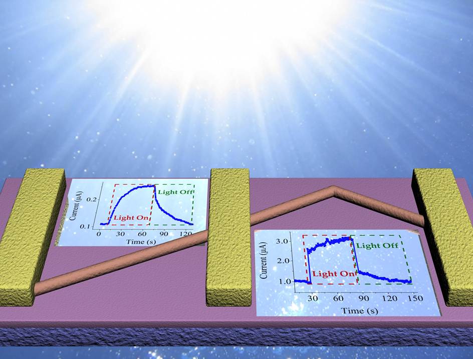
Here we demonstrate a novel and simple geometry-induced high performance of ultraviolet photodetector in which photocurrent and photoresponse speed are both exclusively enhanced by the kinked configuration of single crystalline SnO2 nanowire.Compared with other types of techniques to enhance photoresponse of detector by surface decoration or nanowires crossjunction design, here just a kinked nanowire is required, suggesting an intriguing strategy to simplify the process of device fabrication for high performance of photodetector. More importantly, no external homo/heterogeneous transport barriers were introduced onto surface of SnO2 nanowire, ensuring that the carrier mobility would not influence by scattering. In detail, the kinked point in this structure would enhance the localized surface electric field of nanowire and then work as a localized “gate”, which renders two back-to-back inner homogeneous transport barriers forming, centered at the kinked point, similar as the case of carbon nanotube.15 The localized “gate”, with the help of the inner homogeneous transport barriers, improves the charge separation efficiency and also shorts the transmit time of carriers to electrode, as a result, benefitting the photocurrent and photoresponse of photodetector at the same time.Generally, the photocurrent of kinked nanowire is about 2 to 10 times larger than that of conventional straight nanowire. Surprisingly, the photoresponsivity and external quantum efficiency (EQE) are calculated to be ultrahigh as 1.2×10⁷ A/W and 6.0×10⁹ % at most, respectively. More intriguingly, the photoresponse time of kinked nanowire exhibits a hundred times improvement, compared with straight nanowire case. As such animprovement results exclusively from the geometry of kinked nanowire; it is promising to extend this design into other types of low-dimensional semiconducting materials.